Visual Component Inspection
In the current climate, with components in such short supply, visual quality inspection of goods in, during manufacture, and during the test stages has never been more vital.
High-quality, reliable Printed Circuit Boards (PCBs) control so many products in society today. Sectors such as aerospace, automotive, and medical technology require specialized, performance-critical PCBs, produced in concentrated batches, and obviously, electronic consumer goods and telecommunications equipment manufacturers require a continuous supply of standard PCBs in high volumes.
Aiming to deliver reliable performance and achieve quality targets, manufacturers and their PCB suppliers have rigorous quality assurance procedures in place. Quality Management Systems (QMS) include detailed PCB inspection guidelines, to ensure consistent delivery of high quality products.
A QMS will also include robust reporting requirements, demonstrating a commitment to quality and providing full transparency and traceability in any instances of product failure.
This application note looks at the role manual visual inspection (MVI) plays in the quality management process of PCB manufacture.
What is Manual Visual Inspection?
Manual Visual Inspection (MVI) in PCB manufacture is where an individual examines a PCB and compares it to a ‘Golden Board’ or against detailed quality control criteria contained in the quality control inspection check list. The aim of the visual inspection is to identify any defects before the PCB is integrated into the final product.
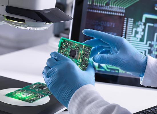
The simplest form of MVI is with the naked eye. However, this is unlikely to identify any but the most obvious defects, particularly when inspecting smaller, more densely packed PCBs. Therefore, more often than not, the board is inspected under a microscope, ensuring a more accurate and detailed view of each element that makes up a functioning PCB.

Inspection during the Design for Manufacturing (DFM) Process
As part of the development stage of New Product Introduction (NPI) many manufacturers outsource the build of their PCB designs to a PCB fabrication company. In the initial prototype stage, the fabricators create an exact replica of the design drawings, perfectly matching every detail of the customer specifications.
At this stage a small test run of the first off board is produced. This is the phase where checks decide whether the design is fit for purpose. Prototypes are inspected under a microscope for any build defects. The PCB is also assessed for possible adaptations that would improve performance or IPC compliance and increase ease and speed of final manufacture.
Once the refined version of the prototype is approved, a larger run of PCBs is produced. Engineering Validation Tests (EVT) and Design Validation Tests (DVT) are conducted. Failure analysis is carried out on PCBs that fail testing and cosmetic checks are also undertaken to ensure boards meet updated client specifications. Any necessary design alterations or amendments to the production process are then made.
Finally, Production Validation Tests (PVT) are run. This is the ‘last build’ stage of the process before the sample PCBs are considered acceptable for mass production.
Throughout the DFM process, a microscope is used for visual inspection, and images captured for inclusion in the NPI documentation.
Continuous inspection is an important part of the PCB DFM process, saving many potential design faults and contributing towards an efficient and cost effective manufacturing process. Therefore, it is important that a high quality inspection system is utilized, offering exceptional image quality and a magnification range that is suitable for the size and intricacy of the PCB being tested.
Reporting throughout the development of the prototype is also important in order to track design changes and document issues found and their resolutions. Capturing of image and video files is part of this reporting process.

Visual Inspection Prior to Product Assembly
On completion of the development process, the approved PCB will move into mass manufacturing. Ahead of this, the necessary components need to be sourced and purchased in the correct quantities.
Often a PCB manufacturer purchases parts from outside suppliers, including electronic sub-assemblies, assembly units and individual components. These items undergo inspection in the Goods In area. Quality control procedures include a detailed list of quality checks to be undertaken and all results recorded alongside captured images of the parts, to ensure full traceability.
Inspection during PCB Mass Manufacturing
The purpose of inspection is to find and fix faults as quickly as possible. To ensure that this happens, creating a well thought out, thorough inspection plan is crucial. PCBs are becoming smaller and more complex as product designs grow ever more sophisticated. This means that inspection processes have become more detailed and complex and need to take place at numerous stages throughout production.
Visual inspection is an important tool in the inspector’s toolbox, with visual comparisons against a ‘Golden Board’ being extremely useful.
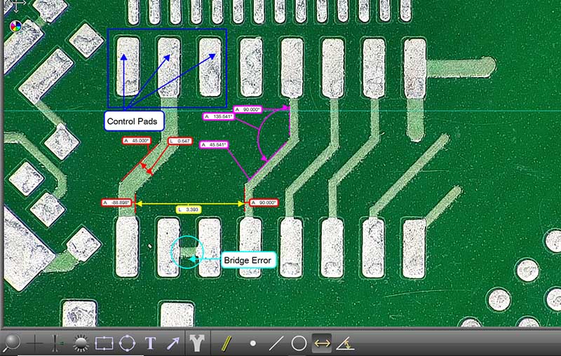
However, it is worth noting that quality control processes include a range of methodologies, meaning visual inspection is often supplemented with other techniques. The simplest of these being the use of overlays, whilst more comprehensive checks may require precise, detailed measurements.
The key to managing detailed inspection
Detailed inspection requirements can increase production times and therefore costs. This is why an effective QMS allows for the batch inspection of regular, low cost components, reserving 100% inspection for performance critical components, where safety is paramount.
Another fundamental criterion for optimizing and reducing the cost of inspection is selecting an inspection system that is easy to use. An intuitive system that requires minimal training, particularly where multiple operators are involved, ensures visual inspection is fast, accurate and consistent.
As mentioned earlier, exceptional image quality and the correct magnification range are key to providing quick and accurate checks.
Finally, a system that allows inspection supervisors to create an efficient workflow through using program pre-sets will maintain accuracy whilst improving throughput.
Common PCB defects looked for during inspection
Component Checks:
Component defects are a major contributor to faulty PCBs, so PCBs need to be checked for the following:
- Missing components
- Misplaced or misaligned components
- Incorrect component value
- Damaged components
- Lifted lead
- Reverted polarity of components
Utilizing additional methods to complement visual inspection, such as overlays and basic measurement software is extremely useful in identifying misaligned components quickly and simply.
In some cases, the ability to obtain an oblique view for a detailed look at an interface or point of intersection on a component can be useful. Rotating the oblique view around the subject adds further clarity of the interface point.
A case in point is when checking the quality of plating on through holes or checking for lifted lead.
Coating Checks:
The integrity of the coating on a PCB is crucial to proper long-term functioning and therefore inspecting coatings is an important part of the process.
Coatings are checked for:
- Pin pricks
- Tears
- Uneven spread
- Thickness
- Correct masking, ensuring coating is only applied to relevant areas on the PCB
The use of illumination when checking coatings is extremely useful in quickly spotting any potential issues. For instance, UV lighting is ideal to assess the integrity of conformal coatings.
Soldering Checks:
One of the key areas to look at during the quality control process on the PCB. Today’s complex boards have thousands of solder joints, all of which are critical to the functioning of the PCB.
Inspectors will check for:
- Solder bridging or shorts
- Any open circuits
- Any voids or bumps
- Residual copper
- Insufficient solder
- Excess solder
- General quality of the soldering
When it comes to speeding up soldering checks, infrared lighting can be used to reduce glare, whilst episcopic illuminators help operators to inspect the plating on through holes.
Throughout all of the quality checks mentioned, inspectors will also be looking at the overall quality of the PCB including looking for any dirt, scratches, dents or warping.
If there is a recurrent fault being reported, manufacturing processes can be altered to resolve this, thereby creating continuous improvement in the manufacturing process and delivering quality assurance for customers.
Our Electronics customers use the following products:
For Inspection
- Mantis eyepiece-less stereo microscope
- Lynx EVO eyepiece-less stereo microscope
- EVO Cam II digital microscope
Measurement
- Swift PRO dual optical and video measurement system
- LVC Series 3 axis measurement systems


